

| << Chapter < Page | Chapter >> Page > |
SSPD_Chapter 1_Part 11_Conclusion_Defects in Crystal structure
1.11.8. CRYSTAL DEFECTS- 1-D DEFECT, 2-D DEFECTS AND 3-D DEFECTS.
A regular array of atoms extending to infinity in all three dimensions is an ideal crystal. In real life , crystals are always surface bounded where we have dangling bonds and hence surface states. Therefore real crystals are never ideal. But apart from this non-ideality, we have externally introduced defects. This could be a missing atom, atoms out of place, irregular arrangement of atoms, irregularity in the spacing of the rows of atoms and the presence of impurities. These defects effect the electrical properties of the material and devices made out of these materials.
Point defects are the simplest category of defects. Vacancies, interstitial impurity atoms and substitutional impurity atoms comprise point defects. They are shown in Figure (1.63). Vacancies and interstitials occur in all crystals due to thermal excitation of 1~2 eV. As the ambient temperature increases the density of such point defects increases. By particle radiation such defects can be purposely introduced in a given sample for specific purposes such as decreasing the lifetime of the minority carriers. The lifetime of minority carriers can be changed from millisecond to pico-seconds. A relatively pure, single and defect-free crystal exhibits millisecond lifetime whereas with introduction of defects it falls. Particle radiation induced defects can kill the lifetime to as low as pico-seconds.
The controlled introduction of impurity dopents influence drift mobility, diffusion coefficient and lifetime. The dopents occupy either interstitial positions or substitutional positions.
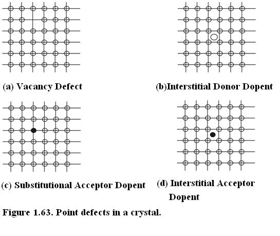
Figure 1.63. Point defects in a crystal.(a)Vacancy, (b) Interstitial Donor Dopent (c) Substitutional Acceptor Dopent, (d) Interstitial Acceptor Dopent;
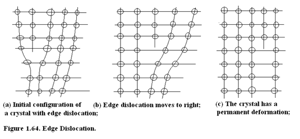
Line Defect(1-D defects) : Dislocations are line defects. These act as precipitate sites for metallic impurities. This degrades the performance of the device.
In edge defect, a line of atoms is not in proper position. This causes a permanent deformation in the crystal structure without the loss of a property called ductility. Metals have the maximum ductility because of the nature of metallic bond. We will discuss the nature of metallic bond in the next section. Edge Defect is illustrated in Figure 1.64.
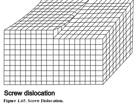
In screw dislocation, a part of the crystal lattice is displaced with respect to the other part. The consequence of this displacement is that atomic layers spiral around this dislocation. Screw Defect is illustrated in Figure 1.65.
Plane Defects(2-D defects) : Solidification of a polycrystalline solid from the melt creates grain boundaries. When crystallographic plane of orientation abruptly changes there we have grain boundaries. Grain Boundaries are shown in Figure 1.66. Grain boundaries lower the mobility of the carriers. Anti-phase boundaries is 2D defect. This occurs in ordered alloy. Here the crystallographic plane direction is the same the layers are in opposite phase. Instead of layer order of ABABABAB…… it is arranged as ABABBABABAB……….Stack faults are also 2-D defect. They occur in a number of crystal structure. But they commonly occur in closed packed structure. Stacking fault is one or two layer interruption in the stacking sequence. Instead of ABCABCABCABC…….. arrangement as found in fcc structure we have ABCABABABC….. arrangements then we say that stacking fault has occurred.
Volume defects(3-D defects): Precipitates and voids are examples. Precipitates are reduced solubility of dopents at reduced temperature. Voids are shown in Figure 1.67
Figure 1.66. Grain Boundaries along with point defects and line defects.
Figure 1.67. Volume Defect such as void.
Notification Switch
Would you like to follow the 'Solid state physics and devices-the harbinger of third wave of civilization' conversation and receive update notifications?

|
|

|
|
|
|
|

|
|

|
|
|
|
|

|
|

|
|
|
|
|

|