

| << Chapter < Page | Chapter >> Page > |
SSPD_CHAPTER 1_Part10_ ELECTRON IN A SINGLE CRYSTAL SOLID AND BAND THEORY OF SOLID.
All solids are present as crystals: either as single crystal or polycrystal or as amorphous.
In gases the molecules are independent of one another and they have no definite shape and no definite volume. They take the shape of the vessel and occupy the total volume of the vessel..
Liquids have definite volume but no definite shape. They take the shape of the vessel they occupy.
Solids are of definite shape and definite volume. In single crystal solids an unit cell of atoms are repeated in all three dimensions to generate the single crystal lattice structure. The unit cells can be cube, face-centered-cube(fcc), body-centered –cube (bcc), rhombic structure or tetrahedral structure.
In single crystals there is long range periodicity in one given orientation. In poly-crystals the periodicity gets interrupted at a short distance of micrometer. Thus poly-crystal is divided in domains. Each domain has its own orientation of periodicity.
Amorphous state has still shorter range of periodicity. Amorphous structure effects the energy band diagram also. In amorphous solids, the band edges are not sharply defined.
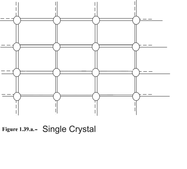
In Figure 1.39.a we illustrate the Single Crystal Structure. Silicon Single Crystal is tetrahedaral structure with 4 electrons in valence orbit completing co-valent bonds with 4 electrons of 4 Si atoms at the corner of the central Si atom. But at the surface of the crystal Si, atoms are not able to complete the co-valent bonds. The incomplete bonds, marked by broken lines, are referred to as ‘Dangling Bonds’. The dangling bonds give rise to surface states . These surface states play a crucial role in Solid State Devices. They can give rise to undesirable leakage current. They can give rise to fluctuating channel conductivity in MOSFET devices. The fluctuating channel conductivity gives rise to Flicker Noise or 1/f noise. These dangling bonds have to be passivated by growing SiO 2 layer. Hence Silicon Dioxide is referred to as Passivation Layer.
In Figure 1.39.b., we illustrate the poly crystal structure. Here we have short range single crystal domains separated by domain boundaries. Each domain has its own crystal orientation. Domain boundary gives rise to scattering and it lowers the mobility of the electron hole carriers. Polycrystal Si is not suitable for producing stable and reproducible devices. But in recent days Poly-Si have been used in selective manner in BJT and in MOSFET to improve the performance of the device as we have seen in the Prologue ( The Journey of IC Technology).
In Figure 1.39.c. we illustrate the amorphous Silicon. As seen they have very short range periodicity and they have many dangling bonds which will give rise to serious problems of reproducibility and stability in device fabrication.
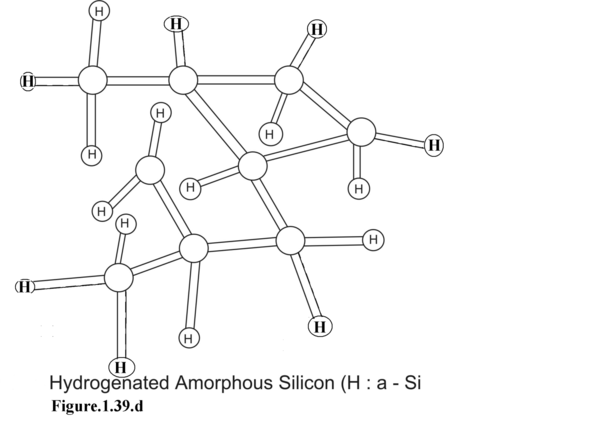
In Figure 1.39.d. hydrogenated amorphous Silicon is shown. Here the dangling bonds have been terminated by Hydrogen co-valent bonds . Saturating the dangling bonds with hydrogenation improves the prospect of using H:a-Si in device fabrication.

In Figure 1.39.c. we see the unsaturated dangling bonds of Si Atoms. This makes the use of a:Si very unreliable in device fabrication.
In Figure 1.39.d. the same unsaturated dangling bonds have been terminated by Hydrogen valence-bond. This enhances the use of H:a-Si in device fabrication.

Figure(1.39) The Three forms of crystalline structure: Single Crystal, Poly-crystal and Amorphous and the hydrogenated a-Si.
In a later Chapter, crystalline structure will be discussed in detail. Here we are concerned with Energy Band Diagram of single crystal.
An electron in free space can occupy a continuum of energy states given by the equation:
E = V(r) + p 2 /(2m) 1.81
But an electron, orbiting around the nucleus of Hydrogen Atom, is permitted to have only discrete energy states as shown in Fig.( 1.40 a).
Equation 1.81 states that when electron is in free space it occupies a continuum of energy states as shown by the parabolic solid line in Figure 1.40.a.
But when the same electron is confined to a potential well, as it is in an Hydrogen atom, then it occupies only discrete energy states expressed by the equation:

This equation was discussed in a previous section Part 7 as Eq 1.35. In Figure 1.40.a it is marked as -13.6eV, -3.4eV, -1.51eV, -0.85eV and -0.544eV for principal quantum numbers n= 1, 2, 3, 4, and 5.
When atoms are arranged into a solid structure, valence and conduction electrons can occupy closely spaced permissible energy states. These permissible energy states are so closely spaced that they appear as a continuous band of permissible energy states. These energy bands are interrupted with energy band gaps. The energy band gaps are forbidden energy states where electrons are not permitted.
The discrete energy states of an electron in a single atom and the permissible energy bands of valence and conduction electrons in a single crystal solid – conductor and insulator are shown in Figure (1.40a,b and c).
Figure 1.40.b. gives the energy band diagram of a conducting solid. As seen in the Figure, conduction band is partially filled and the upper edge of the partially filled band is Fermi Energy Level (E F ). This means Fermi Energy Level is located within the the conduction band. Lower edge of the conduction band is called E C and upper edge of the valence band is E V . Because of available empty energy states in the conduction band, a conductor supports an electric drift current. This is why it is called a conductor.
Figure 1.40.c gives the energy band diagram of an insulator . As seen from the diagram, conduction band is fully empty and valence band is completely filled up. Fermi Energy Level lies exactly in the middle of the Band Gap. If the band gap is greater than 5eV it is a perfect insulator but if E F <5eV then it is a semiconductor above 77Kelvin and below 77Kelvin it continues to be insulator.


Notification Switch
Would you like to follow the 'Solid state physics and devices-the harbinger of third wave of civilization' conversation and receive update notifications?

|
|

|
|

|
|

|
|

|
|

|
|

|
|

|
|

|
|
|
|