

| << Chapter < Page | Chapter >> Page > |
The Onward March of Information Revolution in the second decade of 21 st Century.
Intel’s 22nm Technology moves the transistor into 3 rd Dimension.
In the Journey of IC Technology from Micro to Nano Era we have seen the major developments which have taken place to allow the Moore’s Law to be followed by Industries in IC manufacturing. But as we scale down below 45nm Technology a paradigm shift was inevitable if Moore’s Law is to be obeyed in future.
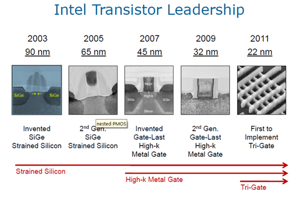
On January 29, 2007, metal gate last and high-K technology in 45nm Technology was introduced. Using this technology Intel Core 2 Duo, Intel Core 2 Quad and multi-core processors were introduced.
On May 4, 2011, Intel introduced Tri-Gate Transistor in 22nm Technology. This was the much awaited paradigm shift which will permit Moore’s Law to be continued for another decade.In conventional 2D MOSFET, a conducting channel is formed in the silicon region below the gate electrode in ON condition. High-K dielectric and metal gate has enabled the sub-threshold current to minimize but it has not completely turned off the channel. Hence power wastage remains though reduced.
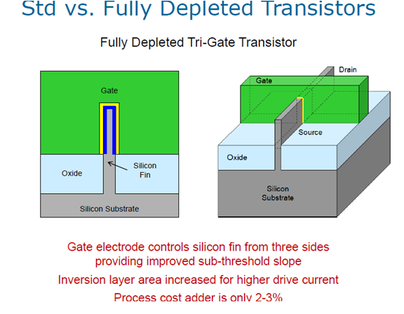
Figure 1. The cross-sectional view and the perspective view of Tri-gate Transistor.
In fully depleted tri-gate transistor, conducting channels are formed on three sides of a vertical fin structure as shown in Figure 1. The additional control (on the sides) enables as much transistor current to flow as possible when the transistor is in the “ON” state and it completely shuts down the current when it in “OFF” condition. This provides unprecedented combination of performance and energy efficiency. Hence it is suitable for a whole range of Computer Applications from servers to desktop and from lap-top to hand-held devices.
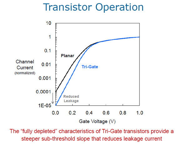
Figure 2. This I-V curve brings out the fully depleted character of Tri-Gate transistors.
This additional control speeds up the toggling rate also. The first microprocessor chip 4004, which had 2300 transistors and which used 10µm technology, toggled at 108kHz. In contrast Tri-Gate Transistor uses 22nm technology and switches 4000 times faster and it cuts down energy consumption by a factor of 1/5000 . The price per transistor has fallen down by a factor of 1/50,000 .
Intel’s 22nm Tri-Gate use third generation high-k/metal-gate scheme, copper interconnects, strained Silicon and 193 nm Immersion Lithography. These terms have been discussed in IC journey from micro to nano era.
Because of heat management considerations 8086 architecture was being gradually replaced by ARM(Advanced RISC Machines) in CPU applications. But the use of 22nm Tri-Gate dramatically changed the energy efficiency scenario as a result 8086 will continue to be in race for CPU applications.
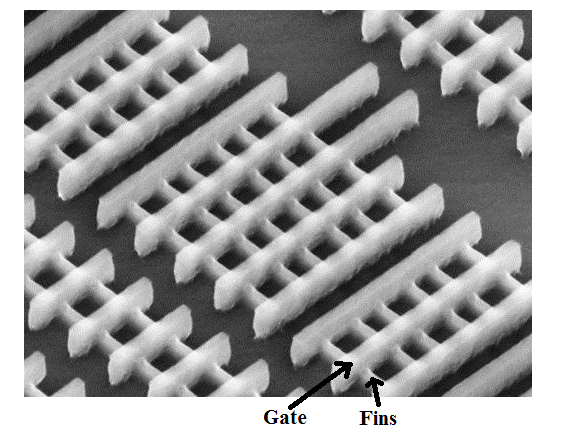
Figure 3. The photo-micrograph of Tri-Gate Transistors based IC.
Intel Technology Road Map.
| Process Name | P1266 | P1268 | P1270 | P1272 | P1274 |
| Lithography | 45nm | 32nm | 22nm | 14nm | 10nm |
| First Production Year | 2007 | 2009 | 2011 | 2013 | 2015 |
Compared to 32nm 2-D transistors, Tri-Gate transistors will be 37% faster and power efficiency will be 50% better. That is for the same operating conditions, Tri-Gate will consume 50% less power. Because of better power efficiency, battery back-up will be prolonged and battery-life will be improved.These will be run at lower voltages. This will also add up to the back-up time as well as the battery life. This will be a boon to heavy-duty network servers.
Tri-Gate transistor is a variant of ‘FinFet’ structure developed by Chenming Hu and his colleagues in late 1990s at University of California, Berkeley. IBM, Samsung and Taiwan Semiconductor Manufacturing Corporation are all working on FinFet. But even this 3-D structure will hit the wall sooner or later. Then perhaps a new technology ‘SPINTRONICS’ will come into picture.
Notification Switch
Would you like to follow the 'Solid state physics and devices-the harbinger of third wave of civilization' conversation and receive update notifications?

|
|

|
|

|
|
|
|
|

|
|

|
|

|
|

|
|

|
|

|