

| << Chapter < Page | Chapter >> Page > |
The Journey of I.C.Technology from micro (1959) to nano (2009) era.-Part 8.
Title: Part 8 and the concluding part of 50 years journey.
Keywords: High K- Metal Gate(HK-MG), Atomic layer deposition, Fermi-Level Pinning(FLP),Strained Silicon,SiGe:C HBT,
Summary: This is the concluding part 8 of 50 years journey.
IV.1.6. High-k solution for ULSI CMOS.[The high-k solution by Mark T. Bohr, Robert S. Chau, Tahir Ghani&Kaizad Mistry, IEEE Spectrum , October 2007, pp 23-29]
As the level of integration evolved, size of CMOS halved every 24 months. At this rate of scaling, by 1998 SiO 2 gate insulation became 5 atomic layer thick with total thickness scaled to 13Aº each atomic layer being 2.6Aº. Current leakage and heating became a serious problem. Because of wave nature of electron and its quantum mechanical tunneling property, thin gate oxides allow the electrons accumulated on gate to leak to the channel. To overcome this problem we need physically thick gate oxides to prevent quantum mechanical tunneling but at the same time electrically thin so that channel is turned at low threshold. If dielectric constant is doubled then thickness can be doubled without any reduction in Turn-ON capability since C=kε 0 A/d
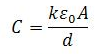
where k=dielectric constant or relative permittivity of the gate insulator
d=thickness of the gate insulator and A= cross-sectional area of the gate insulator.
Metal interconnects are preferred over low-k material so that propagation delay is minimized.
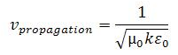
Low k will give higher velocity of propagation thereby minimizing the propagation delay.
MOS capacitance had to be reproducible, its behavior should be repeatable. To achieve this reproducibility and repeatability, Reactive Sputtering or Metal Organic CVD had to be abandoned in favour of Atomic Layer Deposition (Appendix III). This gave the necessary smoothness to the surface of the electrode as well as precise control over the thickness of the Gate Insulator. This ensured reproducibility and repeatability.
Several dielectrics were studied such as Al 2 O 2 , TiO 2 , Ti 2 O 2 , Ti 2 O 5 , HfO 2 , HfSiO 4 , ZrO 2 , ZrSiO 2 , La 2 O 3 .
With scaling due to Fermi-Level pinning (AppendixIV), higher threshold Voltage (V Thres ) resulted. Also High-k material have high elasticity hence result in higher phonon scattering or lattice scattering resulting in lower channel mobility. By screening the phonon effect, the deterioration in channel conductivity ould be prevented. This required by increasing the electron density in Poly-Si gate. Hence we had to switch to Metal-High k combination. This prevented:
In mid-2003, Intel’s Hillsbaro, Ore, Development Fab developed HK-MG CMOS. Intel’s 130nm
technology was used. Using Hafnium-Based Oxide and Metal Gate electrode following characteristics were achieved:
Notification Switch
Would you like to follow the 'Solid state physics and devices-the harbinger of third wave of civilization' conversation and receive update notifications?

|
|

|
|

|
|

|
|

|
|

|
|

|
|

|
|

|
|
|
|