

| << Chapter < Page | Chapter >> Page > |
The Journey of I.C.Technology from micro (1959) to nano (2009) era.-Part 6.
Keywords: Vertical Scaling, Lateral Scaling, transit time, scatter limited velocity;
Summary: This Part 6 of 50 years journey.
IV.1.3.1. The scaling issues in SiGe HBTs.
SiGe successful demonstration was first done in late 1980[Appendix VI,history of HBT]. This was continuously scaled to achieve a record peak f T of 300GHz in 2006[“Effect of collector lateral scaling on performance of high-speed SiGe HBTs with f T >300GHz”, Rieh, Khater, Joseph, Freeman and Ahlgren, IEEE ED Letters, Vol 42, ,No20, 28 th September 2006.]
The speed of operation in vertical devices has two components: transit time across the base and BC reverse biased junction on one hand and RC delays due to junction parasitic and bulk resistances.
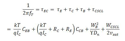
τ E = RC delay time constant at EB junction;
τ C = RC delay time constant at CB junction;
τ B = Transit time delay through Base Width;
τ CSCL = Transit time delay through reverse biased CB junction;
v S = scatter limited velocity of electrons while falling down the potential hill at CB junction;
The vertical scaling is done for reduction in base and collector transit time. This is achieved by reducing the thermal cycles once base profile is achieved. Ge ramp in SiGe base has to be increased and C added to base for limiting the boron diffusion. Ge ramp creates a built-in field which aids the diffusing electrons cross the base region.
To reduce the time delays, base width and collector widths have to be reduced and I C must be increased which requires Kirk Effect should be pushed to higher Current Desities. This achieved by increasing Collector Dopent Concentration. Hence Selectively Implanted Collector(SIC) is introduced.
Lateral scaling reduces the overlap and cross sectional area of the junction hence parasitic capacitance and resistance will be reduced leading to a diminished RC delay time constant. Therefore along with aggressive vertical scaling a judicious lateral scaling also has to be resorted to. Excessive lateral scaling results in an early onset of Kirk effect. So lateral scaling has to be optimized.
Decreasing the Shallow Trench Isolation Width increases the perimeter collector to substrate capacitance which is a significant component in time-delay equation. Hence STI Width is not decreased every generation.
Decreasing the distance between SIC(selectively implanted collector) and extrinsic base implant will increase the overlap i.e. C CB OL. This has to be minimized. This is achieved by raised extrinsic base structure.
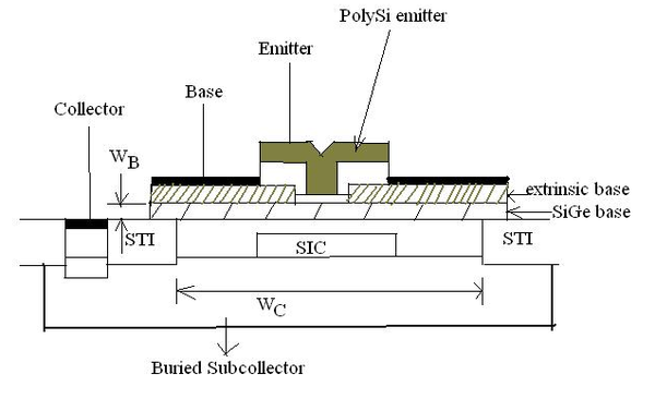
Figure 7. Cross-sectional view of fabricated device.( W B is the base width which is scaled under vertical scaling and W C is the collector width which is scaled under lateral scaling).
The result of aggressive vertical scaling and judicious lateral scaling is shown in the Figure 8.
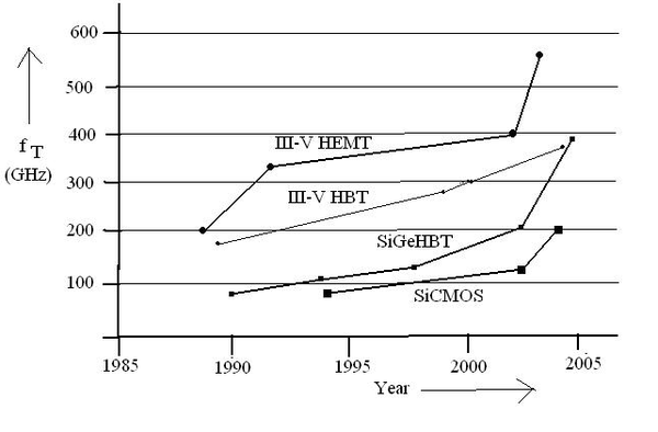
Figure 8. Cutoff frequencies versus year for various Technologies.[Rieh et al, IPRM, 2003, pp374-377]
As is evident from graph in Figure 8, today in 2009 through scaling and innovation , SiGe HBT is a better technology than III-V technology. While trying to improve the performance using scaling technology, some new problems come to the fore namely:
Self heating , electromigration and reduction in the safe region of operation. By scaling the emitter width(E W ) with respect to 1/J C (the peak f T current) significantly reduces self-heating and it eases electromigration problem[“ A look into the Future for SiGe HBTs”, Harame, Freeman et al,IEEE Symposium,WA3.5(invited)]
Heterojunction Bipolar Transistor strategy was adopted to maintain high injection efficiency with high Base conductivity so that base spreading resistance could be minimized and a better figure of merit as well as better f max could be achieved but in practice it is found that as base doping is increased and Ge content and ramp increased, neutral base recombination is enhanced leading to a deterioration in current gain. So an optimization in Ge profile has to be done inorder to get the full advantage of increased base doping[“Current Gain of SiGe HBT under High Base Doping Concentrations” Ningyue Jiang&Zhenquieng Ma,” Semiconductor Science&Technology, 22, S168-S172, 2007.].
SiGe HBT technology was originally developed for high-end computing but it failed because it consumed much more power as compared to that in CMOS. Hence it was abandoned. Subsequently it was found that for RF circuits it consumed much less power as compared to that of CMOS for the same level of performance. So SiGe rapidly developed its application area in various forms of communications such as wired and wireless communication, disk storages, high speed high bandwidth instrumentation. Discrete SiGe are being used universally in RF amplifies and integrated SiGe chips are prolifigating in GSM,CDMA wireless hand sets and base stations. They are rapidly penetrating LAN chipsets and high speed 10-40 Gb/s synchronous optical network(SONET) transceivers.
SiGe real strength lies in its ability to integrate analog, RF and digital on a single chip using existing CMOS fabs. This kind of compatibility is not found with GaAs technology. Apart from this versatility it is enabling new architecture such as direct conversion and software radio.
Today SiGe BiCMOS is the fastest growing semiconductor process.
Notification Switch
Would you like to follow the 'Solid state physics and devices-the harbinger of third wave of civilization' conversation and receive update notifications?

|
|
|
|

|
|

|
|

|
|

|
|

|
|

|
|

|
|

|