

| << Chapter < Page | Chapter >> Page > |
The Journey of I.C.Technology from micro (1959) to nano (2009) era.-Part 5.
Keywords: Bipolar Hetero structure, homo junction, energy band diagram, emitter injection efficiency;
Summary: This part 5 of 50 yrs journey.
IV.1.3. Method of improving Emitter Injection Efficiency by Bipolar Hetero Structure.
I C /I B = β F = [-qAD n . n p (0)| B /W B ]/[ -qAD p . p n (0)| E /W E ] = (W E /W B )(D nB /D pE )(n p (0)| B /p n (0)| E );
But

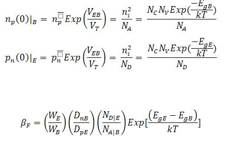
So if the EB junction is not a homojunction but a hetro junction
where (E g | E - E g | B )=0.15eV then β F = 400 even if (N D | E /N A | E ) = 1 that is both E and B are equally doped. But (N D | E /N A | E ) = 1 will drastically reduce Base Spreading Resistance which will leads to improved frequency response as well as improved GBP.
Graphically the improvement is evident as shown in the Graph:
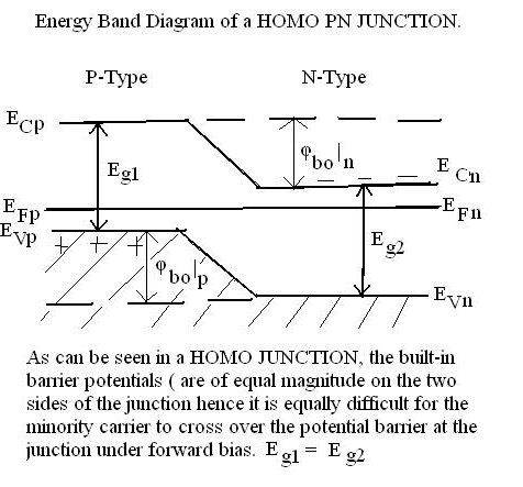
Figure 5. In a HOMO JUNCTION of equal doping on two sides the total forward junction current is made up of 50% electrons being injected from N to P side and 50% holes being injected from P side to N side.
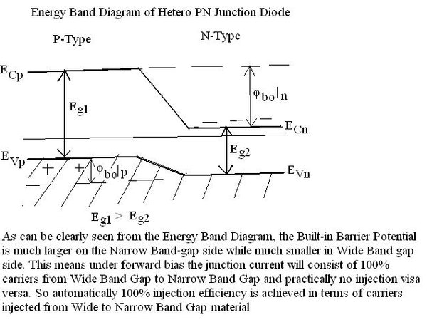
Figure 6. In a HETERO JUNCTION under forward bias the Built-in Barrier Potential are so unequal that Junction Current is wholly constituted of carriers injected from Wide Band Gap to Narrow Band Gap thereby automatically achieving 100% Injection Efficiency even without creating large doping differential on the two sides.
Thus we see that heterojunction are very naturally disposed towards giving 100% injection efficiency even with a very low base spreading resistance.
SiGe Hetro Bipolar Transistors(HBT) hold the key to realizing high speed wire-line and wireless communication circuits and systems.[“Oveview: Fabrication of SiGe HBT&CMOS Technology” edited by Cressler,CRC Press, 2009]
In hetero Junction BJT we have two main contenders:
History of SiGe HBT is given in Appendix VI. In this technology, pseudomorphic Si (1-x) G x layer is used for the base. They are thin films less than 100nm that conform to the lattice pattern of the underlying substrate. This is strained crystalline structure. Carriers have high drift mobility under strained condition. If this film is grown any thicker than 100nm then the stressed film relaxes creating numerous defects and lattice mismatch which renders the film completely useless from device fabrication point of view.
SiGe HBT [Appendix VI] is the child of marriage of Si Technology and Bandgap Engineering Methods of III-V Compund Semiconductor. Only through low temperature Si epitaxy that the alloying of Si&Ge having different band-gaps is possible and doping of such layers with high precision is made possible. SiGe based bandgap engineering is Si Heterostructure Bipolar Technology (SiGe HBT).
SiGe can operate at Cryogenic temperatures whereas BJT freezes out at liquid nitrogen temperature. Hence superior performance parameters can be derived Cryognically cooled SiGe HBT.
SiGe HBT has complete tolerance towards radiation induced damages. Hence it finds very extensive space and interplanetary remote sensing applications. The advantage of low frequency noise of BJT is retained in SiGe HBT.
Though Carbon (C) contamination is very worrisome in minority carrier devices due to deep traps introduced by C, still 0.1 to 0.2% (i.e.10 20 /cm 3) proved to be very beneficial in Si:SiGe:Si devices as it suppressed out diffusion of Base Boron in subsequent thermal cycles.
Notification Switch
Would you like to follow the 'Solid state physics and devices-the harbinger of third wave of civilization' conversation and receive update notifications?

|
|

|
|

|
|

|
|

|
|

|
|

|
|

|
|
|
|
|

|