

| << Chapter < Page | Chapter >> Page > |
The Journey of I.C.Technology from micro (1959) to nano (2009) era.-Part 3.
Title: Part 3 of 50 yrs journey.
Keyword: Scale of Integration, Contact printing, Projection printing, Proximity printing,UV, Deep UV,Immersion Technique.
Summary: This gives Part 3 of 50 yrs journey.
Section III. The Different Generations of Lithographic Technology serving the IC Fabrication Foundries over the last 50 years.
[ “New Uses of IC Technology will enable better opportunities for optical lithography”, Resor&Griff, Solid State Technology,01-Nov07; “Technology Interdependence&the evolution of Semiconductor lithography,” Ron Adner&Rahul Kapur, Solid State Technology, Nov.2007; IC knowledge.com ]
At the time I.C. technology was born mask preparation and optical lithography was manual[Appendix II].
As we move from Small Scale Integrated (SSI) Circuits to Medium Scale Integrated Circuits(MSI) to LSI to VLSI and finally now to ULSI, the need for smaller and smaller feature size in circuit fabrication has driven the evolution of Optical Lithography. Table 5 shows the growth in the packing density of components in the chips fabricated in last 50 years.
Table 5. Classification of Chips according to degree of integration.
| SSI(Small Scale Integrated Circuits) | Less than 30 components |
| MSI(Medium Scale Integrated Circuits) | 30 to 100 components |
| LSI ( Large Scale Integrated Circuits) | 100,000 components |
| VLSI(Very Large Scale Integrated Circuits) | 1 million components |
| ULSI( Ultra Large Scale Integrated Circuits) | 40 million components |
Table 6. The Development in Lithography Technique in last 50 years.
[“Shrinking Possibilities”, Bill Arnold, IEEE Spectrum, April 2009, pp.23-25, 46-48.]
| Year | Generation | W*(nm)Min.linewidth | λ(nm) | Source | Year of dominance | Type of mask | Method of exposure | NumericalAperture |
| 1962 | Contactprinting | 7µm | 480 | UV | 1972 | Emulsionplates | Refraction through lens system | 0.3 |
| Late 60s | Computerization and automation of mask preparation using high speed step and repeat cameras. This gave reduced geometries and greater accuracy. | |||||||
| 1972 | ProximityPrinting. | 3 µm | 480 | UV | 1973 | do | 0.3 | |
| 1973 | Projection | 2µm | 480 | UV | 1977 | Electron beam systems used in mask making | do | 0.3 |
| 1976 | Electron beam | 0.5 µm | 480 | UV | never | . | Electrostaticlensing | 0.3 |
| 1978 | X-Ray | 0.3 µm | 480 | UV | never | No suitable mask materials | ? | 0.3 |
| 1978 | G-line | 1.25 µm | 436 | G line of Hg vap.lamp | 1982 | Lens system.Refractive exposure | 0.3 | |
| 1985 | I-line | 0.80 µm | 436/365 | I line of Hg | 1991 | do | 0.4 | |
| 1986 | DUV248 nm | 0.45 µm | 365 | Same | 1998 | do | 0.4 | |
| 1996 | DUV193nm | 0.15 µm | 365/248 | KrF Excimer | 2006 | do | 0.6 | |
| 1998 | DUV157nm | 0.10 µm | 248 | do | Never | do | 0.6 | |
| 1999 | DUV193nm | 0.18 µm | 248 | do | do | 0.6 | ||
| 2001 | DUV193nm | 0.13 µm | 248 | do | do | 0.7 | ||
| 2003 | DUV193nm | 0.09 µm | 248/193 | ArF Excimer | do | 0.8 | ||
| 2005 | DUV193nm immersion | 0.04 µm | 193 | do | Todate | do | 0.8 | |
| future | EUV 100nm | Less than0.030 µm | Reflective mirror exposure system**. |
W* = minimum feature size=(according to Rayleigh Equation)=k.λ/(NA)
where NA(numerical aperture)=n.Sin(α) = d/(2f);
n= index of refraction of the medium surrounding the lens and α = acceptance angle of the lens system;
d= aperture diameter and f = focal length.
k= resolution factor. Resolution factor is also falling. It depends on the photo resist and resolution enhancement techniques such as :
phase shift mask,
off axis illumination
and optical proximity corrections (this corrects for the blurring effects of diffraction of light from small aperture slits). In the mask a rectangle pattern is replaced by dog bone pattern so that after exposure we get a rectangle with sharp corners on the wafer.
Increased NA gives reduced depth of focus. For high resolution, surface of Photoresist must be flat and within the depth of focus.
By looking at the Rayleigh Equation we immediately see the advantage of using immersion technique. The most suitable medium is non-ionized ultra pure water which has n=1.47 and absorption less than 6% over 6mm. This medium is non-contaminating hence most suitable for immersion optical lithography. By immersion technology, DUV 157nm will be able to go up to minimum line width of less than 30nm.
** The mask and the refractive lens used in conventional lithography systems would absorb 100nm light required for patterning features smaller than 50 nm. Hence refractive lens is replaced by reflective mirror and masks are replaced by reflecting type Molybednum-Silicon masks a few nm’s thick . On this a pattern of chromium is laid down. This absorbs light in appropriate places and reflects elsewhere and thus the pattern is transferred to the Wafer.
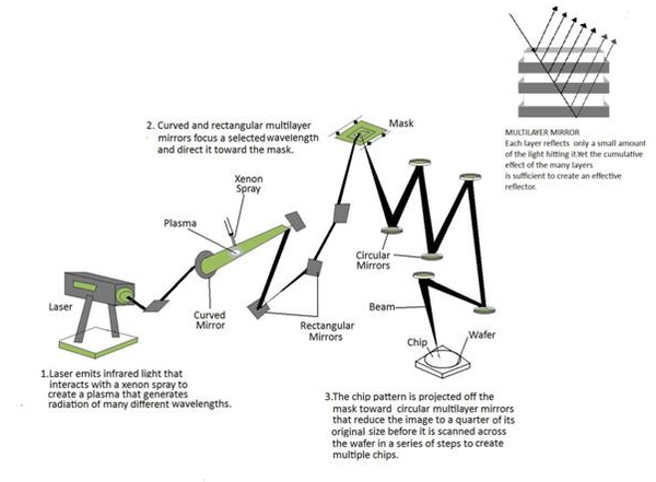
Figure 3. Extreme UltraViolet Lithography.
[Curtsey Scientific American , April 2004, The First Nanochips by G.Dan Hutcheson]
At 100nm and below Optical Lithography reaches its limit even with Resolution Enhancement Techniques such as Optical Proximity Corrections and Phase Shift Masks. So we have to work out Post Optical Lithgraphy or Next Generation Lithography. SAMATECH Program has come up with five alternatives for NGL. These are described in Appendix II.
Notification Switch
Would you like to follow the 'Solid state physics and devices-the harbinger of third wave of civilization' conversation and receive update notifications?

|
|

|
|

|
|

|
|

|
|

|
|

|
|

|
|

|
|

|