

| << Chapter < Page | Chapter >> Page > |
The Journey of I.C.Technology from micro (1959) to nano (2009) era.-Part 2.
Title: Part 2 of 50 yrs journey.
Keywords: Isolation Diffusion, base stripe geometry, buried layer, vertical scaling and lateral scaling.
Summary: This Part 2 of 50 yrs journay.
Section I. The Bipolar Junction Transistor Technology in 60’s-70’s.
In 1959 at the time IC Technology was invented, the vertical NPN transistor looked as given in Figure 1.
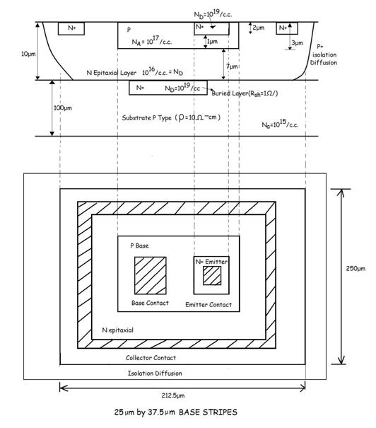
Figure 1. Cross-sectional View and plan view of Vertical NPN transistor.
(25um by 37.5um base stripe geometry)
Total area covered 212 μm by 250 μm
Substrate is 100um thick.
Epitaxial layer is 10um thick.
Base Collector Junction is at 3um depth and Emitter-Base Jn. at 2um depth.
Hence Base Width = W B = 1 um thick.
P Substrate- ρ=10Ω-cm, N A = 10 15 Boron atoms/cc;
Buried Layer has been put to reduce Collector Series Resistance.
N D =10 19 Arsenic Atoms/cc; In buried layer Arsenic is used as donor type dopent because it has much lower diffusion coefficient hence almost negligible out diffusion in subsequent diffusion and heating cycles.
N Epitaxial layer- ρ= 0.1Ω-cm, N D = 10 16 Phosphorous Atoms/cc;
Base layer- N A = 10 17 Boron Atoms/cc; Base layer has a sheet resistance of 200Ω/sq.
Emitter and Collector Contact layer- N D = 10 19 Phosphorous Atoms/cc, R sh = 1Ω/sq;
Section II. The Bipolar Junction Transistor Technology in 1980’s-2000’s.
Gordon Moore is a co-founder of Intel and he made an empirical observation which became a Law . It stated :
“ at our rate of technological development, the complexity of an integrated circuit, with respect to minimum component cost will double in about 24 months”.[“Cramming more components onto Integrated Circuits”, Electronics Magazine, 19 April 1965]. The law has held the test of time to date as is evident from Table I.4.
Today Moore’s Law has become a self fulfilling prophecy and a goal Industry tries to achieve all the time. In attempting to maintain this rate of growth enormous R&D has gone into the development of tools and equipments required for IC fabrication and into the advancement of processing techniques required for IC fabrication.
IC Fabrication has two major parts :
1. System/circuit design and I.C. layout of the components;
2. Photolithographic Masks preparation
3. Actual fabrication of the IC chip.
The actual fabrication consists of the following steps:
During fabrication, suitable windows have to be etched in SiO 2 layer grown over the wafer. By the use of optical lithographic techniques, proper patterns are etched out using a suitable mask for selective diffusion or selective ion-implantation. This step is repeated at buried layer diffusion/implantation, at isolation diffusion, at base diffusion, emitter&collector contact diffusion and at metallization step.
Obeying Moore’s law requires continuous scaling of the I.C. components and hence working at smaller and smaller feature size at the minimum cost. The main burden of this challenge falls on Mask Making and Lithography Techniques. Therefore the continuous and relentless march of IC from micron dimensions to nano dimensions has meant continuous improvement and breakthroughs in Lithography Technology. In fact lithography technology is the major enabling technology in IC Chips fabrication.
In Table 2 , Table 3 and Table 4 we show how the dimensions have been scaled down over the past decades in both Bipolar and MOS Technology. In 1966 emulsion mask patterns were contact printed on 200mm wafer with the smallest feature size of 25µm. In 2007 using Deep Ultra Violet(DUV)193nm immersion Lithography, 30nm ±6nm feature size are imprinted on 300mm wafer.
Table 2. Transistor Junction Depths and Doping Changes with years. [Muller&Kamini, Solid State Devices; “Modelling of SiGe heterojunction transistors:200GHz frequencies with symmetrical delay times”, Jochen Eberhardt&Erich Kasper, Solid State Electronics, 45(2001), 2097-2100.].
| Amplifying(Junction. Isolated)1964 | Amplifying(Junction Isolated)1980 | Switching(Junction Isolated)1980 | Switching(Oxide Isolated)1980 | Amplifying(oxide isolated)2001HBT | |
| Surface area | 212.5µm×250µm | 20 µm×1µm | |||
| Epi Film ThicknessResistivity of epi layer | 10 μm0.1Ω-cm | 10μm1Ω-cm | 3μm0.3-0.8 Ω-cm | 1.2um0.3-0.8 Ω-cm | 172nmW C = 50nm |
| Buried Layer Sheet R Sheet Updiffusion | 1Ω/▄2.5 μm | 20Ω/▄2.5μm | 20Ω/▄1.4μm | 30 Ω/▄0.3 μm | 0.7 Ω/▄0 μm |
| Emitter Diffusion DepthSheet Resistance of Emitter | 2.5 μm1Ω/▄ | 2.5μm5Ω/▄ | 0.8μm12Ω/▄ | 0.25μm30Ω/▄ | W E = 110nm378 Ω/▄Emitter contact5.2 Ω/▄ |
| Base Diffusion DepthR SHEET | 3.5 μm200Ω/▄ | 3.25μm100 Ω/▄ | 1.3μm200 Ω/▄ | 0.5μm600 Ω/▄ | 122nm260 Ω/▄ |
| Base Width | 1 μm | 1 μm | 0.5 μm | 0.25 μm | W B =12nm |
| Substrate ResistivityCrystal Orientation | 10 Ω-cm<111> | 10 Ω-cm<111> | 10 Ω-cm<111> | 5 Ω-cm<111> |
Table 3. Dimension Scaling in MOSFET over the last decade.
| MOS | 1967 | 1997 | 1999 | 2001 | 2003 | 2006 |
| L(µm) | 10 | 0.25 | 0.18 | 0.13 | 0.1 | 0.07 |
| DRAM (Gbit/cm 2 ) | 64M | 0.18 | 0.38 | 0.42 | 0.91 | 1.85 |
| Junction Depth (x j )nm | 1000 | 100 | 70 | 60 | 52 | 40 |
| InterconnectionPitch(nm) | 2000 | 600 | 500 | 350 | 245 | 130 |
International Technology Roadmap for Semiconductors uses ‘nodes’ to refer to the smallest feature size on Logic Chips. This is the width of the gate of MOSFET. Whereas in Memory Chips ‘half pitch’ is used to define the smallest feature size. Half Pitch is half the distance between two adjacent aluminum interconnections. Nodes and Half pitch are illustrated in Figure 2.
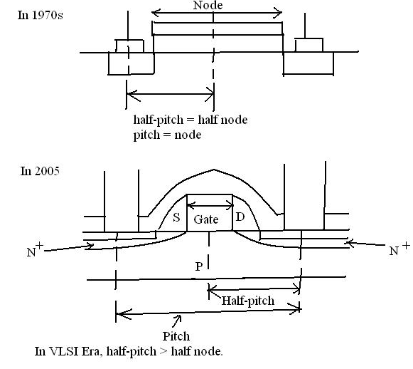
Figure 2. Illustration of the definition of node and pitch.
In 2005, gate width is 32nm, node is 65nm and half pitch is 105nm.
In 2009:
| Logic Chip | Memory Chip | |
| Half-pitch | 50/56nm | 34nm |
| Node | 32nm | 22nm |
Table 4. Scaling in IC Chips in terms of half pitch and nodes.
| Year | Node(nm) | Half-pitch(nm) | Gate- length*(nm) |
| 2009 a | 32 | 52 | 29 |
| 2007 a | 45 | 68 | 38 |
| 2005 b | 65 | 90 | 32 |
| 2004 b | 90 | 90 | 37 |
| 2003 b | 100 | 100 | 45 |
| 2001 c | 130 | 150 | 65 |
| 1999 c | 180 | 230 | 140 |
| 1997 d | 250 | 250 | 200 |
| 1995 d | 350 | 350 | 350 |
| 1992 d | 500 | 500 | 500 |
* The physical length has become smaller than printed length.
As feature size has reduced, shorter wave length has to be used hence light source in Lithography will have to be changed. If the printing feature is smaller than wavelength then light tends to get diffracted and edges get blurred. By image enhancement techniques, smaller feature size can be achieved with larger wavelength.
Now we will examine how Lithography Technology has evolved over the last 50 years.
Notification Switch
Would you like to follow the 'Solid state physics and devices-the harbinger of third wave of civilization' conversation and receive update notifications?

|
|

|
|

|
|

|
|

|
|

|
|

|
|

|
|

|
|

|