

| << Chapter < Page | Chapter >> Page > |
Appendix VIII.
Mobility enhancement in strained Silicon.
[Mobility Enhancement, the next vector to extend Moore’s Law, Nidhi Mohata&Scott E. Thompson, IEEE Circuits&Devices Magazine, September/October 2005, pp.18-23]
Geometric Scaling has been driving IC Industry till date. Since 90-nm Technology generation was introduced, off-state leakage current and power density have made scaling a difficult and challenging job. New scaling vectors were adopted to meet this challenge. At 90-nm generation, mobility enhancement through uniaxial process-induced strained Si has emerged as the next scaling vector.
The theoretical formulations of carriers in 2-D inversion layer just below the insulator Gate:
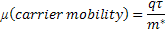
where τ is the mean free time between two consecutive scatterings;
1/τ = scattering rate;
m * is the conductivity effective mass.
Under strain, both m * and scattering rate reduce leading to enhanced mobility.
Uniaxial stress always provide higher current enhancement(1.46mA/µm and 0.88mA/µm for n-channel and p-channel respectively) as compared to that produced by biaxial stress(0.85mA/µm and 0.45mA/µm for n-channel and p-channel respectively). Hence in state of art technologies, Industries have adopted uniaxial stress. There are three state-of-art techniques:
VIII.1. First Approach of local epitaxial film.
The process flow is shown in Figure VIII.1. As shown first Si source and drain are etched, creating an Si recess.
In next step, SiGe (for p-channel) or SiC ( for n-channel) is grown in the source and drain region. This creates uniaxial compressive stress in p-channel or uniaxial tensile stress in n-channel MOSFET. 17%Ge, gives 500-900MPa of channel stress. 60 to 90% drive current enhancements on short cannel devices(~35nm) have been demonstrated. This is greater than that achieved in multigates or high-k dielectrics.
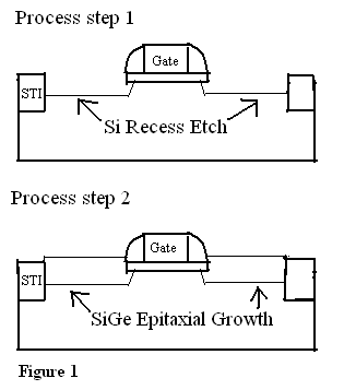
Figure VIII.1. Process Flow of local epitaxial growth.
VIII.2.Second Approach of the use of a tensile and/or compressive capping layer.
The process flow of the second approach is shown in Figure V.2.
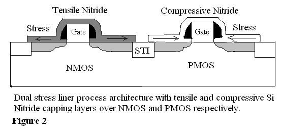
Figure VIII.2. Process Flow of Dual Capping with permanent layer.
In the second approach, capping films are introduced as a permanent layer post salicide. STI is shallow trench isolation.
VIII.3. Third Approach of capping with sacrificial layer.
In the third approach , an uniform layer of high tensile Si 3 N 4 liner is deposited over the entire surface post salicidation. This is patterned and etched so that capping is removed from PMOS and is retained over NMOS. Next a compressive SiN is deposited over the entire surface and selectively patterned and etched off from NMOS. Thus Compressive Nitride is retained over PMOS. This produces comparable stresses as compared to the first approach at the same time it has reduced process complexity and integration issues.
VIII.4. Fourth Approach of Stress Memorization of Poly-Si Gate.
In the fourth approach, the following is the process steps:
After removal of the capping layer the memory of stress is retained in the gate as well as channel.
This is able to enhance the mobility by 10% in NMOS..
Future Scalability of Strain.
In long channel devices:

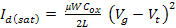
As we scale down, short channel effect start showing up until MOSFET carrier transport becomes ballistic. Under Ballistic transport saturation drain current is described by the following equation:

Where<v(0)>is the average velocity at the source;

In the limit, where channel length becomes zero and electrons or holes are ballistically thrown across the pinched off region, there<v(0)>= unidirectional thermal velocity = v
T =


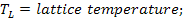
Therefore

Transverse effective mass continues to be reduced by strain hence drain saturation current will be enhanced even under ballistic transport condition which prevails under short channel condition. This will be more the case as the device is scaled. Thus strain will continue to scale well even in future generations as MOSFET goes deeper in Ballistic Mode of Transport.
Notification Switch
Would you like to follow the 'Solid state physics and devices-the harbinger of third wave of civilization' conversation and receive update notifications?

|
|

|
|

|
|

|
|
|
|
|

|
|

|
|
|
|
|

|
|

|