

| << Chapter < Page | Chapter >> Page > |
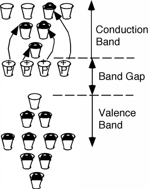
To see how we can make silicon a useful electronic material, we will have to go back to its crystal structure ( [link] ). Suppose somehow we could substitute a few atoms of phosphorus for some of the silicon atoms.

If you sneak a look at the periodic table, you will see that phosphorus is a group V element, as compared with silicon whichis a group 14(IV) element. What this means is the phosphorus atom has five outer or valenceelectrons, instead of the four which silicon has. In a lattice composed mainly of silicon, the extra electron associated withthe phosphorus atom has no "mating" electron with which it can complete a shell, and so is left loosely dangling to thephosphorus atom, with relatively low binding energy. In fact, with the addition of just a little thermal energy (from thenatural or latent heat of the crystal lattice) this electron can break free and be left to wander around the silicon atom freely.In our "energy band" picture, we have something like what we see in [link] . The phosphorus atoms are represented by the added cups with P's on them. They are newallowed energy levels which are formed within the "band gap" near the bottom of the first empty band. They are located closeenough to the empty (or "conduction") band, so that the electrons which they contain are easily excited up into theconduction band. There, they are free to move about and contribute to the electrical conductivity of the sample. Notealso, however, that since the electron has left the vicinity of the phosphorus atom, there is now one more proton than there areelectrons at the atom, and hence it has a net positive charge of 1 q . We have represented this by putting a little "+" sign in each P-cup. Note that thispositive charge is fixed at the site of the phosphorous atom called a donor since it "donates" an electron up into the conduction band, and is not free to move about in thecrystal.
How many phosphorus atoms do we need to significantly change the resistance of our silicon? Suppose we wanted our 1 mm by 1 mmsquare sample to have a resistance of one ohm as opposed to more than 60 MΩ. Turning the resistance equation around we get, [link] . And hence, if we continue to assume an electron mobility of 1000 cm 2 /volt.sec, [link] .
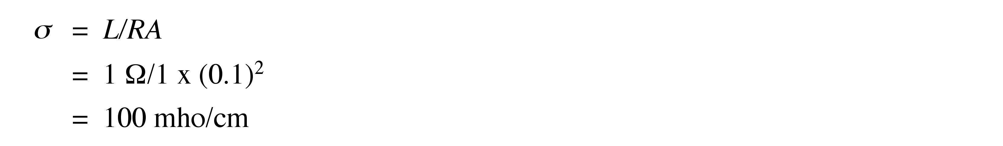

Now adding more than 6 x 10 17 phosphorus atoms per cubic centimeter might seem like a lot of phosphorus, until you realize that there are almost 10 24 silicon atoms in a cubic centimeter and hence only one in every 1.6 million silicon atoms has to be changed into aphosphorus one to reduce the resistance of the sample from several 10s of MΩ down to only one Ω. This is the realpower of semiconductors. You can make dramatic changes in their electrical properties by the addition of only minute amounts ofimpurities. This process is called doping the semiconductor. It is also one of the great challenges of the semiconductormanufacturing industry, for it is necessary to maintain fantastic levels of control of the impurities in the material inorder to predict and control their electrical properties.
Notification Switch
Would you like to follow the 'Chemistry of electronic materials' conversation and receive update notifications?

|
|

|
|

|
|

|
|

|
|

|
|

|
|

|
|

|
|

|