

| << Chapter < Page | Chapter >> Page > |
CRYSTAL GROWTH
Silicon, (Si) :The most common semiconductor, atomic number 14,
energy gap Eg= 1.12 eV- indirect bandgap;
crystal structure- diamond, lattice constant 0.543 nm,
atomic concentration 5 x 10 22 atoms/cm -3 ,
index of refraction 3.42, density 2.33 g/cm 3 , dielectric constant 11.7,
intrinsic carrier concentration 1.02 x 10 10 cm -3 ,
bulk mobility of electrons and holes at 300°K: 1450 and 500 cm 2 /V-s,
thermal conductivity 1.31 W/cm°C,
thermal expansion coefficient 2.6 x 10 -6 °C -1 ,
melting point 1414°C; excellent mechanical properties (MEMS applications);
single crystal Si can be processed into wafers up to 300mm in diameter.
In future this diameter will be 450mm.
P type= Always Boron (B) Doped N type= Dopant typically as follows:Res: .001-.005 Arsenic (As)Res: .005-.025 Antimony (Sb)Res:>.1 Phosphorous (P)
EPITAXIAL CRYSTAL GROWTH
The substrate or the wafer only constitutes the strong base of the integrated circuit. The actual active and passive components fabrication and there integration are carried out in overlay films which are grown by epitaxial technique.
EPITAXY is a Greek word meaning : ‘epi’ (upon)&‘taxy’ (ordered). That is an epitaxial film, a few μm thick, is an orderly continuation of the substrate crystal. It grows very slowly layer by layer. Hence the dimension , defects and doping magnitude as well as uniformity can be precisely and accurately controlled in the crystal growth direction.
This precise control is obtained in Molecular Beam Epitaxy (MBE) but not in Liquid Phase Epitaxy(LPE) or in Chemical Vapour Phase Epitaxy (CVPE). The thickness accuracy is within ±3À which is essential for growing Quantum Photonic Devices namely Quantum Dots, Quantum Wells and Super-lattices
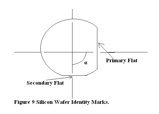
Table 2. Identity marks of the Wafer to identify its orientation and semiconductor type.
| α (angle between primary and secondary flats as indicated in Figure 9) | Type | Orientation |
| 45º | N | <111> |
| 90º | P | <100> |
| 180º | N | <100> |
| 0º | P | <111> |
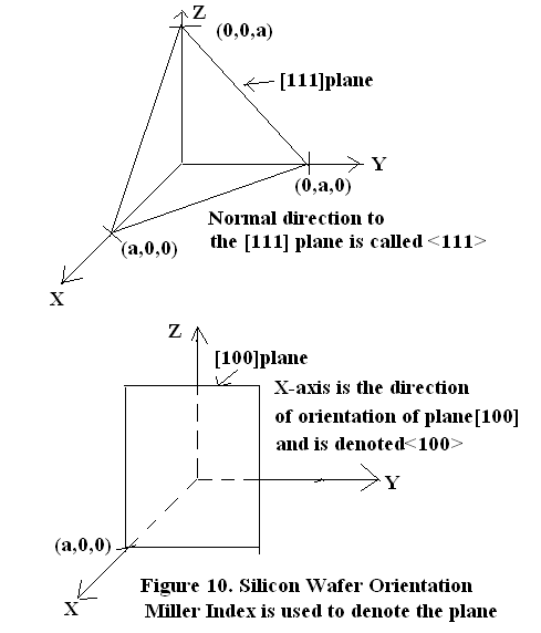
The normal to the plane along which crystals cleaves is the cleavage plane orientation. Suppose the cleavage plane orientation is<111>. Miller Index is being used to define the planes and their normal. Figure 10 illustrates the Plane’s Miller Index and how the normal to the plane is represented. If the exposed surface of the Si wafer, which is known as major flat, is parallel to cleavage plane then the given wafer has a crystal orientation<111>.
If the cleavage plane orientation is<100>and the wafer major flat is parallel to YZ plane then the crystal orientation is<100>. In this case cleavage plane lies in YZ plane i.e. [100] plane and its orientation is perpendicular to YZ plane i.e. x-axis. Hence Wafer Crystal Plane orientation is<100>
Scribing the wafer along cleavage planes allows it to be easily diced into individual chips (‘die”) so that billions of individual circuits or systems on an average wafer can be separated into individual dies. Each individual die is eutectic ally bonded on ceramic substrate. The substrate is bonded to the header.The gold wire is connected to the bonding pads of the die on one end and to the chip terminals on the header by Thermo-compression bonding or by Ultra-sonic bonding. Next the die is hermetically sealed into Dual-in-Line(DIP) package or TO5 package
In<100>crystal orientation, scribed pieces form rectangle whereas in<111>crystal orientation, scribed pieces form triangles. Here we have to scribe from the base of the triangle to the apex.
For MOS fabrications, wafers with crystal orientation<100>are used. This helps achieve a lower threshold voltage. For BJT and other applications wafers with orientation<111>are preferred.
Silicon Crystal Bulk is isotropic to diffusion of dopents and to etchents used for etching the oxide layer. This is because of the symmetric property of Cubic Structure of Si. But real devices are built near the surface hence the orientation of the crystal does matter.
In 111 crystal terminates on 111 plane and in 100 it terminates on 100 plane. 111 plane has largest number of Si atoms per cm2 whereas 100 has the least number of atoms per cm2. Because of this difference 111 planes oxidize much faster because the oxidation rate is proportional to the Silicon atoms available for reaction.
But because the atom surface density is the highest the dangling bond surface density is also the highest in 111 hence Si/SiO2 has superior electrical properties in terms of interface states in 100. Interface states give rise to 1/f noise or flicker noise. Because of this superiority all MOS devices use 100 crystal orientation. But historically BJT have used 111 because 111 crystal growth is easier to grow by Czochralski method. But as we move to sub-micron and deep and ultra-deep sub-micron BJT, 100 crystal orientation seems to be the crystal orientation of choice for BJT also.
Notification Switch
Would you like to follow the 'Electrical and electronic materials science' conversation and receive update notifications?

|
|

|
|

|
|

|
|

|
|

|
|

|
|

|
|

|
|

|