

| << Chapter < Page | Chapter >> Page > |
As previously mentioned, QDs are small enough that quantum effects influence their properties. At sizes under approximately 10 nm, quantum confinement effects dominate the optoelectronic properties of a material. Quantum confinement results from electrons and electron holes being squeezed into a dimension that approaches a critical quantum measurement, called the exciton Bohr radius. As explained above, the distance between the electron and the hole within an exciton is called the exciton Bohr radius. In bulk semiconductors the exciton can move freely in all directions, but when the size of a semiconductor is reduced to only a few nanometers, quantum confinement effects occur and the band gap properties are changed. Confinement of the exciton in one dimension produces a quantum well, confinement in two dimensions produces a quantum wire, and confinement in all three dimensions produces a quantum dot.
Recombination occurs when an electron from a higher energy level relaxes to a lower energy level and recombines with an electron hole. This process is accompanied by the emission of radiation, which can be measured to give the band gap size of a semiconductor. The energy of the emitted photon in a recombination process of a QD can be modeled as the sum of the band gap energy, the confinement energies of the excited electron and the electron hole, and the bound energy of the exciton as show in [link] .
The confinement energy can be modeled as a simple particle in a one-dimensional box problem and the energy levels of the exciton can be represented as the solutions to the equation at the ground level (n = 1) with the mass replaced by the reduced mass. The confinement energy is given by [link] , where ħ is the reduced Plank’s constant, µ is the reduced mass, and a is the particle radius. m e and m h are the effective masses of the electron and the hole, respectively.
The bound exciton energy can be modeled by using the Coulomb interaction between the electron and the positively charged electron-hole, as shown in [link] .The negative energy is proportional to Rydberg’s energy ( R y ) (13.6 eV) and inversely proportional to the square of the size-dependent dielectric constant, ε r . µ and m e are the reduced mass and the effective mass of the electron, respectively.
Using these models and spectroscopic measurements of the emitted photon energy (E), it is possible to measure the band gap of QDs.
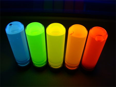
Photoluminescence (PL) Spectroscopy is perhaps the best way to measure the band gap of QDs. PL spectroscopy is a contactless, nondestructive method that is extremely useful in measuring the separation between different energy levels. PL spectroscopy works by directing light onto a sample, where energy is absorbed by electrons in the sample and elevated to a higher energy-state through a process known as photo-excitation. Photo-excitation produces the electron-electron hole pair. The recombination of the electron-electron hole pair then occurs with the emission of radiation (light). The energy of the emitted light (photoluminescence) relates to the difference in energy levels between the lower (ground) electronic state and the higher (excited) electronic state. This amount of energy is measured by PL spectroscopy to give the band gap size.
Notification Switch
Would you like to follow the 'Nanomaterials and nanotechnology' conversation and receive update notifications?

|
|

|
|

|
|

|
|

|
|

|
|

|
|

|
|

|
|

|