

| << Chapter < Page | Chapter >> Page > |
We can show that γ is defined by the relation by a more advanced treatment, [link] .
After substituting the value of I 0 given by [link] into [link] , we take the napierian logarithm of the two sides and multiply them by kT for large forward bias (qV>3kT); thus, rearranging, we have [link] .
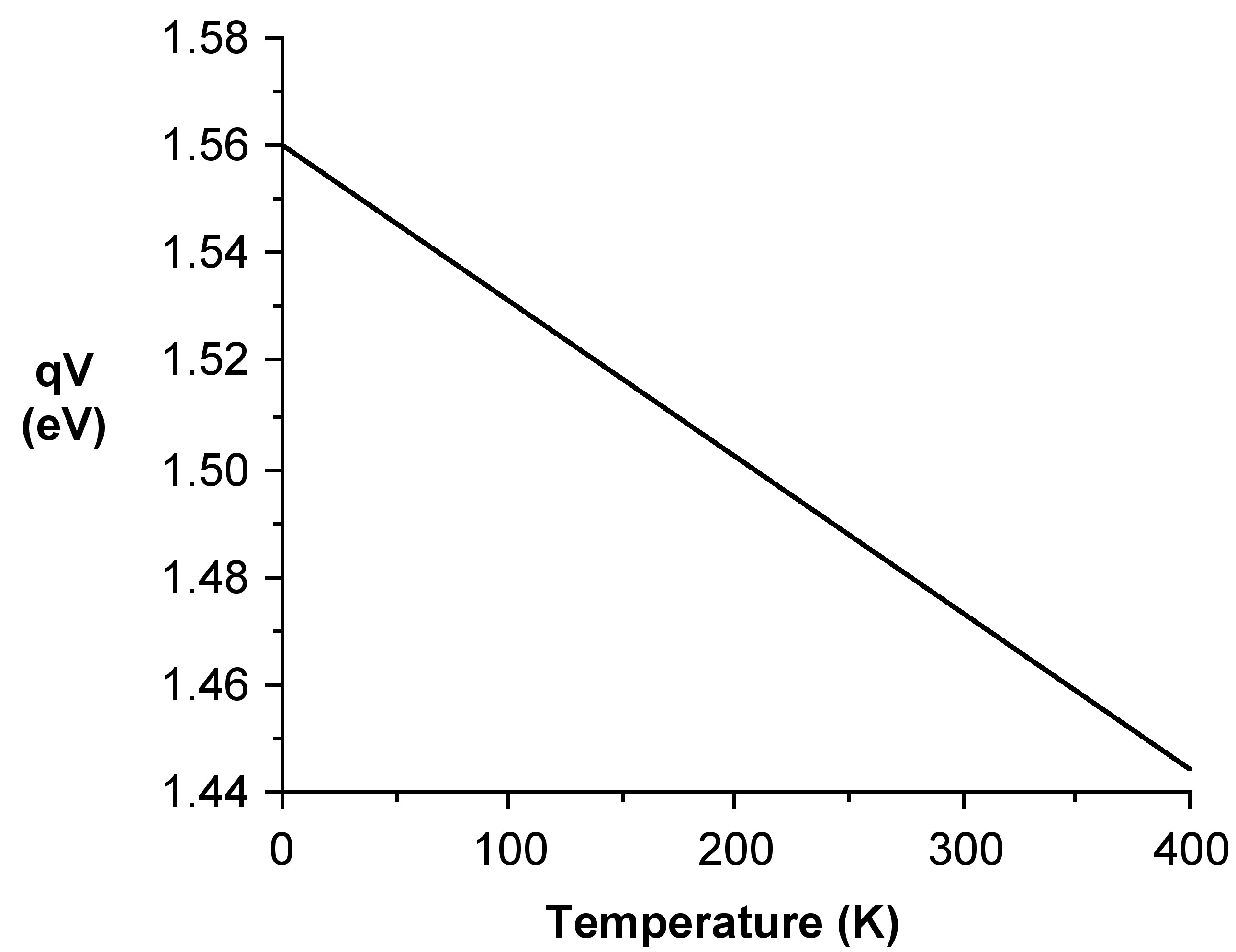
As InT can be considered as a slowly varying function in the 200 - 400 K interval, therefore for a constant current, I, flowing through the junction a plot of qV versus the temperature should approximate a straight line, and the intercept of this line with the qV axis is the required value of the band gap E g extrapolated to 0 K. Through [link] instead of qV, we can get a more precise value of Eg.
[link] shows that the value of γ depends on the temperature and µ that is a very complex function of the particular materials, doping and processing. In the 200 - 400 K range, one can estimate that the variation ΔE g produced by a change of Δγ in the value of γ is [link] . So a rough value of γ is sufficient for evaluating the correction. By taking the experimental data for the temperature dependence of the mobility µ, a mean value for γ can be found. Then the band gap energy qV can be determined.
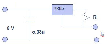
The electrical circuit required for the measurement is very simple and the constant current can be provided by a voltage regulator mounted as a constant current source (see [link] ). The potential difference across the junction can be measured with a voltmeter. Five temperature baths were used: around 90 °C with hot water, room temperature water, water-ice mixture, ice-salt-water mixture and mixture of dry ice and acetone. The result for GaAs is shown in [link] . The plot qV corrected (qV c ) versus temperature gives E 1 = 1.56±0.02 eV for GaAs. This may be compared with literature value of 1.53 eV.
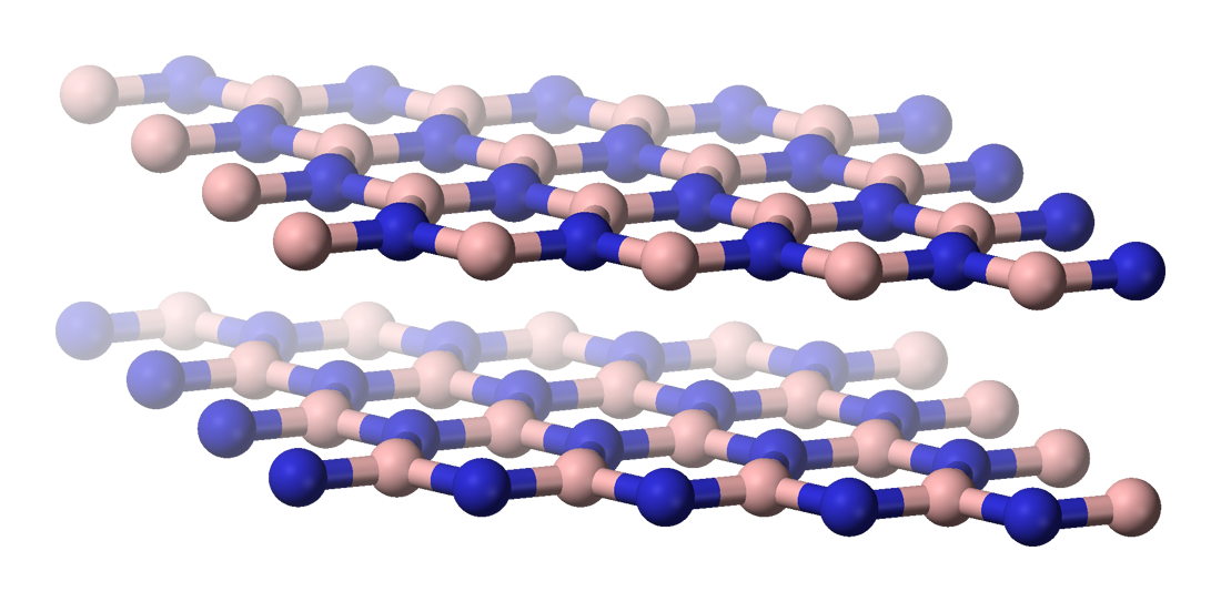
Optical method can be described by using the measurement of a specific example, e.g., hexagonal boron nitride (h-BN, [link] ). The UV-visible absorption spectrum was carried out for investigating the optical energy gap of the h-BN film based on its optically induced transition.
For this study, a sample of h-BN was first transferred onto an optical quartz plate, and a blank quartz plate was used for the background as the reference substrate. The following Tauc’s equation was used to determine the optical band gap E g , [link] , where ε is the optical absorbance, λ is the wavelength and ω = 2 π / λ is the angular frequency of the incident radiation.
As [link] a shows, the absorption spectrum has one sharp absorption peak at 201 - 204 nm. On the basis of Tauc’s formulation, it is speculated that the plot of ε 1/2 / λ versus 1/ λ should be a straight line at the absorption range. Therefore, the intersection point with the x axis is 1/ λ g ( λ g is defined as the gap wavelength). The optical band gap can be calculated based on E g ) hc / λ g . The plot in [link] b shows ε 1/2 / λ versus 1/ λ curve acquired from the thin h-BN film. For more than 10 layers sample, he calculated gap wavelength λ g is about 223 nm, which corresponds to an optical band gap of 5.56 eV.
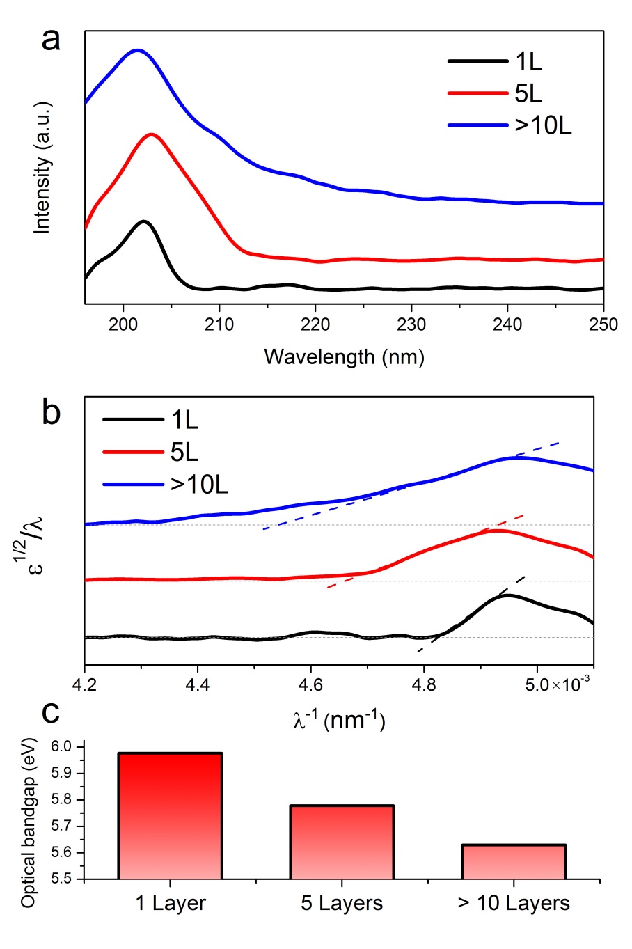
Previous theoretical calculations of a single layer of h-BN shows 6 eV band gap as the result. The thickness of h-BN film are 1 layer, 5 layers and thick (>10 layers) h-BN films, the measured gap is about 6.0, 5.8, 5.6 eV, respectively, which is consistent with the theoretical gap value. For thicker samples, the layer-layer interaction increases the dispersion of the electronic bands and tends to reduce the gap. From this example, we can see that the band gap is relative to the size of the materials, this is the most important feature of nano material.
Notification Switch
Would you like to follow the 'Nanomaterials and nanotechnology' conversation and receive update notifications?

|
|

|
|

|
|

|
|
|
|
|
|
|
|

|
|

|
|

|
|

|