

| << Chapter < Page | Chapter >> Page > |
Before understanding the electronic structure of a quantum dot semiconductor, it is important to understand what a quantum dot nanoparticle is. We earlier studied that a nanoparticle is any particle with one of its dimensions in the 1 - 100 nm. A quantum dot is a nanoparticle with its diameter on the order of the materials exciton Bohr radius. Quantum dots are typically 2 - 10 nm wide and approximately consist of 10 to 50 atoms. With this understanding of a quantum dot semiconductor, the electronic structure of a quantum dot semiconductor can be described by the following terms.
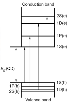
When the size of the semiconductor crystal becomes comparable or smaller than the exciton Bohr radius, the quantum dots are in a state of quantum confinement. As a result of quantum confinement, the energy levels in a quantum dot are discrete ( [link] ) as opposed to being continuous in a bulk crystal ( [link] ).
In materials that have small number of atoms and are considered as quantum confined, the energy levels are separated by an appreciable amount of energy such that they are not continuous, but are discrete (see [link] ). The energy associated with an electron (equivalent to conduction band energy level) is given by is given by [link] , where h is the Planck’s constant, m e is the effective mass of electron and n is the quantum number for the conduction band states, and n can take the values 1, 2, 3 and so on. Similarly, the energy associated with the hole (equivalent to valence band energy level) is given by [link] , where n' is the quantum number for the valence states, and n' can take the values 1, 2, 3, and so on. The energy increases as one goes higher in the quantum number. Since the electron mass is much smaller than that of the hole, the electron levels are separated more widely than the hole levels.
As seen from [link] and [link] , the energy levels are affected by the diameter of the semiconductor particles. If the diameter is very small, since the energy is dependent on inverse of diameter squared, the energy levels of the upper edge of the band gap (lowest conduction band level) and lower edge of the band gap (highest valence band level) change significantly with the diameter of the particle and the effective mass of the electron and the hole, resulting in a size dependent tunable band gap. This also results in the discretization of the energy levels.
Qualitatively, this can be understood in the following way. In a bulk semiconductor, the addition or removal of an atom is insignificant compared to the size of the bulk semiconductor, which consists of a large number of atoms. The large size of bulk semiconductors makes the changes in band gap so negligible on the addition of an atom, that it is considered as a fixed band gap. In a quantum dot, addition of an atom does make a difference, resulting in the tunability of band gap.
Notification Switch
Would you like to follow the 'Nanomaterials and nanotechnology' conversation and receive update notifications?
|
|

|
|

|
|

|
|

|
|

|
|

|
|

|
|

|
|

|