

| << Chapter < Page | Chapter >> Page > |
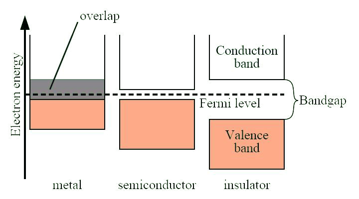
In solid state physics a band gap also called an energy gap, is an energy range in an ideal solid where no electron states can exist. As shown in [link] for an insulator or semiconductor the band gap generally refers to the energy difference between the top of the valence band and the bottom of the conduction band. This is equivalent to the energy required to free an outer shell electron from its orbit about the nucleus to become a mobile charge carrier, able to move freely within the solid material.
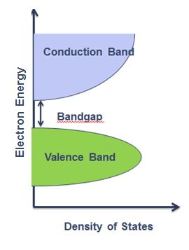
The band gap is a major factor determining the electrical conductivity of a solid. Substances with large band gaps are generally insulators (i.e., dielectric), those with smaller band gaps are semiconductors, while conductors either have very small band gaps or no band gap (because the valence and conduction bands overlap as shown in [link] ).
The theory of bands in solids is one of the most important steps in the comprehension of the properties of solid matter. The existence of a forbidden energy gap in semiconductors is an essential concept in order to be able to explain the physics of semiconductor devices. For example, the magnitude of the bad gap of solid determines the frequency or wavelength of the light, which will be adsorbed. Such a value is useful for photocatalysts and for the performance of a dye sensitized solar cell.
Nanocomposites materials are of interest to researchers the world over for various reasons. One driver for such research is the potential application in next-generation electronic and photonic devices. Particles of a nanometer size exhibit unique properties such as quantum effects, short interface migration distances (and times) for photoinduced holes and electrons in photochemical and photocatalytic systems, and increased sensitivity in thin film sensors.
For a p-n junction, the essential electrical characteristic is that it constitutes a rectifier, which allows the easy flow of a charge in one direction but restrains the flow in the opposite direction. The voltage-current characteristic of such a device can be described by the Shockley equation, [link] , in which, I 0 is the reverse bias saturation current, q the charge of the electron, k is Boltzmann’s constant, and T is the temperature in Kelvin.
When the reverse bias is very large, the current I is saturated and equal to I 0 . This saturation current is the sum of several different contributions. They are diffusion current, generation current inside the depletion zone, surface leakage effects and tunneling of carriers between states in the band gap. In a first approximation at a certain condition, I 0 can be interpreted as being solely due to minority carriers accelerated by the depletion zone field plus the applied potential difference. Therefore it can be shown that, [link] , where A is a constant, E g the energy gap (slightly temperature dependent), and γ an integer depending on the temperature dependence of the carrier mobility µ.
Notification Switch
Would you like to follow the 'Nanomaterials and nanotechnology' conversation and receive update notifications?

|
|

|
|

|
|

|
|

|
|

|
|

|
|

|
|

|
|

|