

| << Chapter < Page | Chapter >> Page > |
The purpose of wafering is to saw the crystal into thin slices with precise geometric dimensions. By far, the most common method of wafering semiconductor crystals is the use of an annular, or inner diameter (ID), diamond saw blade. A schematic diagram of ID slicing technology is shown in [link] .
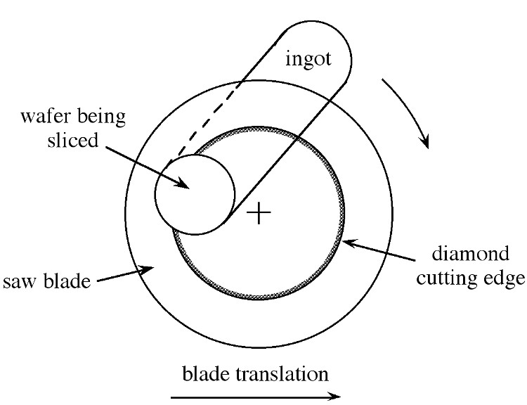
The crystal, when it arrives at the sawing area, has been ground to diameter, flatted, and etched. In order to slice it, the crystal must be firmly mounted in such a way that it can be completely converted to wafers with minimum waste. The crystal is attached with wax or epoxy to a mounting block, which is usually cylindrical in shape and of the same diameter as the ingot. Also, a mounting beam (or strip) is attached along the length of the crystal at the breakout point of the saw blade. This reduces exit chipping (breakage that occurs as the blade exits the crystal at the end of a cut) and also provides support for the sawn wafer until it is retrieved. Graphite or phenolic resins are common materials for the mounting block and beams, although some success has been obtained in mounting ingots using hydraulic pressure. The saw blade is a thin sheet of stainless steel (325 μm), with diamond bonded to its inner edge. This blade is mounted on a drum that rotates at
Both silicon and GaAs crystals are grown with either the crystallographic<100>or<111>direction parallel to the cylindrical axis of the crystal. Wafers may be cut either exactly perpendicular to the crystallographic axis or deliberately off-axis by several degrees. In order to obtain the proper wafer orientation, the crystal must be properly oriented on the saw. All production slicing machines have adjustments for orientation of the crystal; however, it is usually necessary to check the orientation of the first slice in order to assure that all subsequent slices will be properly oriented.
Obvious variables introduced during the wafering process include: cutting rate, wheel speed, and coolant flow rate. However, the condition of the machines, such as alignment and vibration, is the most important variable followed by the condition of the blade. A deviated blade rim may cause taper, bow, or warp. [link] summarizes the types of deformations that can occur during wafering, their physical appearance and their characteristics.
Notification Switch
Would you like to follow the 'Chemistry of electronic materials' conversation and receive update notifications?

|
|

|
|

|
|
|
|

|
|

|
|

|
|

|
|

|
|

|