

| << Chapter < Page | Chapter >> Page > |
The first step in oxidizing a surface of silicon is the removal of the native oxide which forms due to exposure to open air. This may seem redundant to remove an oxide only to put on another, but this is necessary since uncertainty exists as to the purity of the oxide which is present. The contamination of the native oxide by both organic and inorganic materials (arising from previous processing steps and handling) must be removed to prevent the degradation of the essential electrical characteristics of the device. A common procedure uses a H 2 O-H 2 O 2 -NH 4 OH mixture which removes the organics present, as well as some group I and II metals. Removal of heavy metals can be achieved using a H 2 O-H 2 O 2 -HCl mixture, which complexes with the ions which are formed. After removal of the native oxide, the desired oxide can be grown. This growth is useful because it provides: chemical protection, conditions suitable for lithography, and passivation. The protection prevents unwanted reactions from occurring and the passivation fills vacancies of bonds on the surface not present within the interior of the crystal. Thus the oxidation of the surface of silicon fulfills several functions in one step.
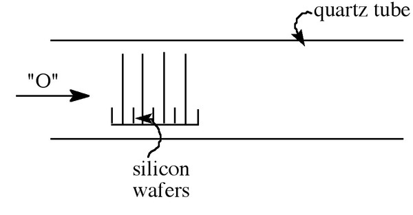
The growth of oxides on a silicon surface can be a particularly tedious process, since the growth must be uniform and pure. The thickness wanted usually falls in the range 50 - 500 Å, which can take a long time and must be done on a large scale. This is done by stacking the silicon wafers in a horizontal quartz tube while the oxygen source flows over the wafers, which are situated vertically in a slotted paddle (boat), see [link] . This procedure is performed at 1 atm pressure, and the temperature ranges from 700 to 1200 °C, being held to within ±1 °C to ensure uniformity. The choice of oxidation technique depends on the thickness and oxide properties required. Oxides that are relatively thin and those that require low charge at the interface are typically grown in dry oxygen. When thick oxides are required (>0.5 mm) are desired, steam is the source of choice. Steam can be used at wide range of pressures (1 atm to 25 atm), and the higher pressures allow thick oxide growth to be achieved at moderate temperatures in reasonable amounts of time.
The thickness of SiO 2 layers on a Si substrate is readily determined by the color of the film. [link] provides a guidline for thermal grown oxides.
| Film thickness (μm) | Color | Film thickness (μm) | Color |
| 0.05 | tan | 0.63 | violet-red |
| 0.07 | brown | 0.68 | "bluish" |
| 0.10 | dark violet to red-violet | 0.72 | blue-green to gree |
| 0.12 | royal blue | 0.77 | "yellowish" |
| 0.15 | light blue to metallic blue | 0.80 | orange |
| 0.17 | metallic to light yellow-green | 0.82 | salmon |
| 0.20 | light gold | 0.85 | light red-violet |
| 0.22 | gold | 0.86 | violet |
| 0.25 | orange to melon | 0.87 | blue violet |
| 0.27 | red-violet | 0.89 | blue |
| 0.30 | blue to violet blue | 0.92 | blue-green |
| 0.31 | blue | 0.95 | yellow-green |
| 0.32 | blue to blue-green | 0.97 | yellow |
| 0.34 | light green | 0.99 | orange |
| 0.35 | green to yellow-green | 1.00 | carnation pink |
| 0.36 | yellow-green | 1.02 | violet red |
| 0.37 | green-yellow | 1.05 | red-violet |
| 0.39 | yellow | 1.06 | violet |
| 0.41 | light orange | 1.07 | blue-violet |
| 0.42 | carnation pink | 1.10 | green |
| 0.44 | violet-red | 1.11 | yellow-green |
| 0.46 | red-violet | 1.12 | green |
| 0.47 | violet | 1.18 | violet |
| 0.48 | blue-violet | 1.19 | red-violet |
| 0.49 | blue | 1.21 | violet-red |
| 0.50 | blue green | 1.24 | carnation pink to salmon |
| 0.52 | green | 1.25 | orange |
| 0.54 | yellow-green | 1.28 | "yellowish" |
| 0.56 | green-yellow | 1.32 | sky blue to green-blue |
| 0.57 | "yellowish" | 1.40 | orange |
| 0.58 | light orange to pink | 1.46 | blue-violet |
| 0.60 | carnation pink | 1.50 | blue |
Notification Switch
Would you like to follow the 'Chemistry of electronic materials' conversation and receive update notifications?

|
|

|
|

|
|

|
|

|
|
|
|
|

|
|
|
|
|
|
|
|

|