

| << Chapter < Page | Chapter >> Page > |
Address space
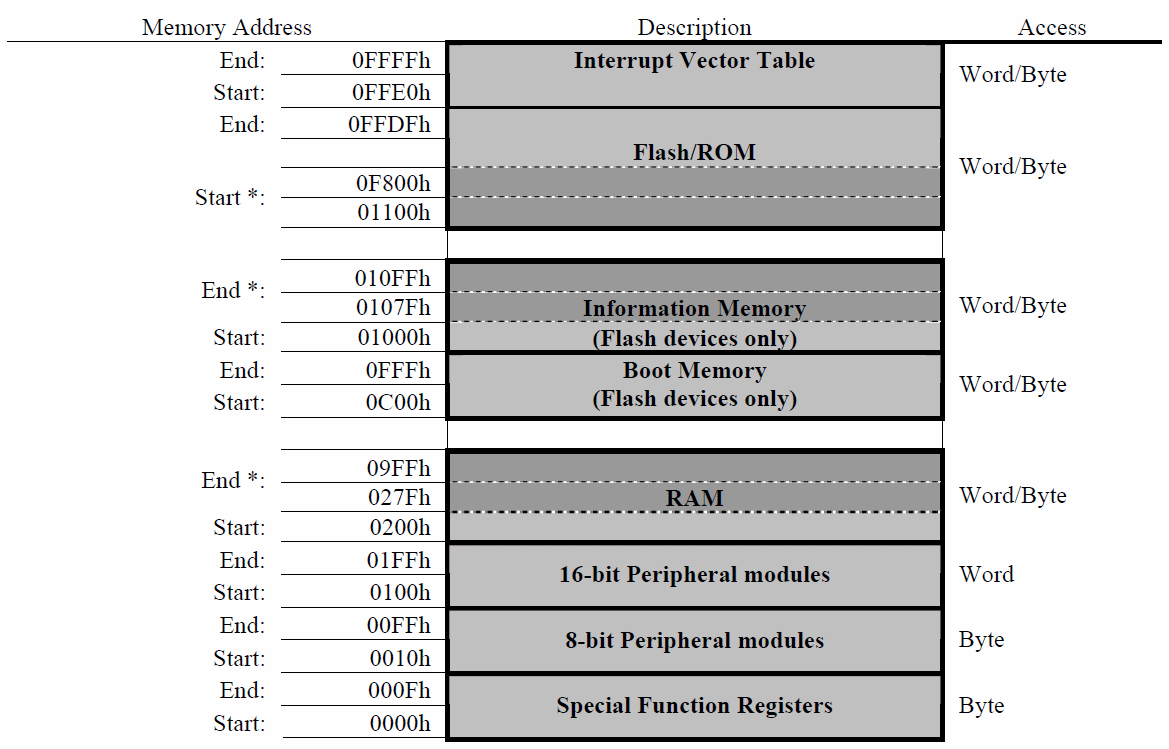
All memory, including RAM, Flash/ROM, information memory, special function registers (SFRs), and peripheral registers are mapped into a single, contiguous address space.
Note: See the device-specific datasheets for specific memory maps. Code access is always performed on even addresses. Data can be accessed as bytes or words.
The MSP430 is available with either Flash or ROM memory types. The memory type is identified by the letter immediately following “MSP430” in the part numbers.
Flash devices : Identified by the letter “F” in the part numbers, having the advantage that the code space can be erased and reprogrammed.
ROM devices : Identified by the letter “C” in the part numbers. They have the advantage of being very inexpensive because they are shipped pre-programmed, which is the best solution for high-volume designs.
For all devices, each memory location is formed by 1 data byte. The CPU is capable of addressing data values either as bytes (8 bits) or words (16 bits). Words are always addressed at an even address, which contain the least significant byte, followed by the next odd address, which contains the most significant byte. For 8-bit operations, the data can be accessed from either odd or even addresses, but for 16-bit operations, the data values can only be accessed from even addresses.
The interrupt vector table is mapped at the very end of memory space (upper 16 words of Flash/ROM), in locations 0FFE0h through to 0FFFEh (see the device-specific datasheets). The priority of the interrupt vector increases with the word address.
Interrupt vector table for MSP430 families.
| Vector Address | Priority | ’ 11xx and ’ 12xx | ’ 13x and ’ 14x | ‘2xx | ’ 3xx | ’ 4xx |
| 0xFFFE | 31, Highest | Hard Reset/ Watchdog | Hard Reset/ Watchdog | Hard Reset/ Watchdog | Hard Reset/ Watchdog | Hard Reset/ Watchdog |
| 0xFFFC | 30 | Oscillator/ Flash/NMI | Oscillator/ Flash/NMI | Oscillator/ Flash/NMI | Oscillator/ Flash/NMI | Oscillator/ Flash/NMI |
| 0xFFFA | 29 | Unused | Timer_B | Timer_B (22x2, 22x4, 23x, 24x, 26x only) | Dedicated I/O | Timer_B(’43x and’44x only) |
| 0xFFF8 | 28 | Unused | Timer_B | Timer_B (22x2, 22x4, 23x, 24x only) | Dedicated I/O | Timer_B(’43x and’44x only) |
| 0xFFF6 | 27 | Comparator | Comparator | Comparator_A+ (20x1 only, 21x1, 23x, 24x, 26x) | Unused | Comparator |
| 0xFFF4 | 26 | Watchdog Timer | Watchdog Timer | Watchdog Timer+ | Watchdog Timer | Watchdog Timer |
| 0xFFF2 | 25 | Timer_A | USART Rx | Timer_A | Timer_A | USART0 Rx(’43x and’44x only) |
| 0xFFF0 | 24 | Timer_A | USART0 Tx | Timer_A | Timer_A | USART0 Tx(’43x and’44x only) |
| 0xFFEE | 23 | USART0 Rx (’12xx only) | ADC | USCI Rx(22x2, 22x4, 23x, 24x, 26x only)I2C status (23x, 24x) | USART Rx | ADC(’43x and’44x only) |
| 0xFFEC | 22 | USART0 Tx (’12xx only) | Timer_A | USCI Tx(22x2, 22x4, 23x, 24x, 26x only)I2C Rx/Tx (23x, 24x, 26x only) | USART Tx | Timer_A |
| 0xFFEA | 21 | ADC10 | Timer_A | ADC10 (20x2 22x2, 22x4 only)ADC12 (23x, 24x, 26x only)SD16_A (20x3 only) | ADC(’32x and ’33x) Timer/Port (’31x) | Timer_A |
| 0xFFE8 | 20 | Unused | Port 1 | USI(20x2, 20x3 only) | Timer/Port(’32x and ’33x) | Port 1 |
| 0xFFE6 | 19 | Port 2 | USART1 Rx | Port P2 | Port 2 | USART1 Rx(’44x only) |
| 0xFFE4 | 18 | Port 1 | USART1 Tx | Port P1 | Port 1 | USART1 Tx(’44x only) |
| 0xFFE2 | 17 | Unused | Port 2 | USCI Rx (23x, 24x, 26x only)I2C status (241x, 261x only) | Basic Timer | Port 2 |
| 0xFFE0 | 16 | Unused | Unused | USCI Tx (23x,24x only)I2C Rx/Tx (241x, 261x only) | Port 0 | Basic Timer |
| 15 | DMA (241x, 261x only) | |||||
| 14 | DAC12 (241x, 261 only) | |||||
| 13 to 0Lowest | Reserved |
The start address of Flash/ROM depends on the amount of Flash/ROM present on the device. The start address varies between 01100h (60k devices) to 0F800h (2k devices) and always runs to the end of the address space at location 0FFFFh. Flash can be used for both code and data. Word or byte tables can also be stored and read by the program from Flash/ROM.
All code, tables, and hard-coded constants reside in this memory space.
The MSP430 flash devices contain an address space for information memory. It is like an onboard EEPROM, where variables needed for the next power up can be stored during power down. It can also be used as code memory. Flash memory may be written one byte or word at a time, but must be erased in segments. The information memory is divided into two 128-byte segments. The first of these segments is located at addresses 01000h through to 0107Fh (Segment B), and the second is at address 01080h through to 010FFh (Segment A). This is the case in 4xx devices. It is 256 bytes (4 segments of 64 bytes each) in 2xx devices.
The MSP430 flash devices contain an address space for boot memory, located between addresses 0C00h through to 0FFFh. The “bootstrap loader” is located in this memory space, which is an external interface that can be used to program the flash memory in addition to the JTAG. This memory region is not accessible by other applications, so it cannot be overwritten accidentally. The bootstrap loader performs some of the same functions as the JTAG interface (excepting the security fuse programming), using the TI data structure protocol for UART communication at a fixed data rate of 9600 baud.
RAM always starts at address 0200h. The end address of RAM depends on the amount of RAM present on the device. RAM is used for both code and data.
Peripheral modules consist of all on-chip peripheral registers that are mapped into the address space. These modules can be accessed with byte or word instructions, depending if the peripheral module is 8-bit or 16-bit respectively. The 16-bit peripheral modules are located in the address space from addresses 0100 through to 01FFh and the 8-bit peripheral modules are mapped into memory from addresses 0010h through to 00FFh.
Some peripheral functions are mapped into memory with special dedicated functions. The Special Function Registers (SFRs) are located at memory addresses from 0000h to 000Fh, and are the specific registers for:
- Interrupt enables (locations 0000h and 0001h);
- Interrupt flags (locations 0002h and 0003h);
- Enable flags (locations 0004h and 0005h).
SFRs must be accessed using byte instructions only. See the device-specific data sheets for the applicable SFR bits.
Request the MSP430 Teaching ROM Materials here (External Link)
Notification Switch
Would you like to follow the 'Teaching and classroom laboratories based on the “ez430” and "experimenter's board" msp430 microcontroller platforms and code composer essentials' conversation and receive update notifications?

|
|

|
|

|
|

|
|

|
|

|
|

|
|

|
|

|
|

|