

| << Chapter < Page | Chapter >> Page > |
As long as design requirements are met, the input-outputrelation for the inverting amplifier also applies when the feedback and input circuit elements are impedances (resistors,capacitors, and inductors).
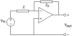
Let's design an op-amp circuit that functions as a lowpassfilter. We want the transfer function between the output and input voltage to be where equals the passband gain and is the cutoff frequency. Let's assume that the inversion (negative gain) does not matter. With the transfer functionof the above op-amp circuit in mind, let's consider some choices.
Creating a specific transfer function with op-amps does not have a unique answer. As opposed to design with passive circuits,electronics is more flexible (a cascade of circuits can be built so that each has little effect on the others; see [link] ) and gain (increase in power and amplitude) can result. To complete our example,let's assume we want a lowpass filter that emulates what the telephone companies do. Signals transmitted over the telephonehave an upper frequency limit of about 3 kHz. For the second design choice, we require . Thus, many choices for resistance and capacitance values arepossible. A 1 μF capacitor and a 330 Ω resistor, 10 nF and 33 kΩ, and 10 pF and 33 MΩ wouldall theoretically work. Let's also desire a voltage gain of ten: , which means . Recall that we must have . As the op-amp's input impedance is about 1 MΩ, we don'twant too large, and this requirement means that the last choice forresistor/capacitor values won't work. We also need to ask for less gain than the op-amp can provide itself. Because thefeedback "element" is an impedance (a parallel resistor capacitor combination), we need to examine the gainrequirement more carefully. We must have for all frequencies of interest. Thus, . As this impedance decreases with frequency, the designspecification of means that this criterion is easily met. Thus, the first two choices for the resistor and capacitor values (as well as manyothers in this range) will work well. Additional considerations like parts cost might enter into thepicture. Unless you have a high-power application (this isn't one) or ask for high-precision components, costs don't dependheavily on component values as long as you stay close to standard values. For resistors, having values , easily obtained values of are 1, 1.4, 3.3, 4.7, and 6.8, and the decades span 0-8.
What is special about the resistor values; why these rather odd-appearing values for ?
The ratio between adjacent values is about .
When we meet op-amp design specifications, we can simplify our circuit calculations greatly, so much so that we don't needthe op-amp's circuit model to determine the transfer function. Here is our inverting amplifier.
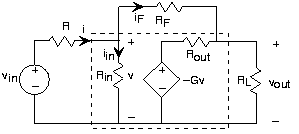
When we take advantage of the op-amp'scharacteristics—large input impedance, large gain, and small output impedance—we note the two followingimportant facts.
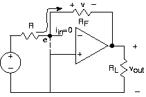
Armed with these approximations, let's return to our original circuit as shown in [link] . The node voltage is essentially zero, meaning that it is essentially tied tothe reference node. Thus, the current through the resistor equals . Furthermore, the feedback resistor appears in parallel withthe load resistor. Because the current going into the op-amp is zero, all of the current flowing through flows through the feedback resistor( )! The voltage across the feedback resistor equals . Because the left end of the feedback resistor is essentiallyattached to the reference node, the voltage across it equals the negative of that across the output resistor: .Using this approach makes analyzing new op-amp circuits much easier. When using this technique, check to make sure theresults you obtain are consistent with the assumptions of essentially zero current entering the op-amp and nearly zerovoltage across the op-amp's inputs.

Let's try this analysis technique on a simple extension of the inverting amplifier configuration shown in [link] . If either of the source-resistor combinations were notpresent, the inverting amplifier remains, and we know that transfer function. By superposition, we know that theinput-output relation is
What utility does this circuit have? Can the basic notion of the circuit be extended without bound?
Notification Switch
Would you like to follow the 'Fundamentals of electrical engineering i' conversation and receive update notifications?

|
|
|
|
|

|
|

|
|

|
|

|
|

|
|

|
|

|
|

|
|

|
|

|